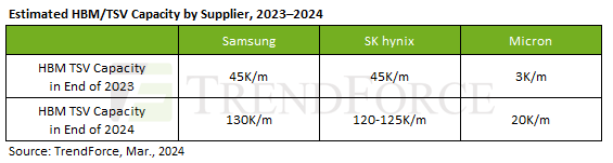
By the end of 2024, the DRAM industry is expected to have allocated approximately 250K/m (14%) of total capacity to producing HBM TSV, with an estimated annual supply bit growth of around 260%, says TrendForce svp Avril Wu.
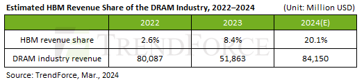
HBM’s revenue share within the DRAM industry—around 8.4% in 2023—is projected to increase to 20.1% by the end of 2024.
The die size of HBM is generally 35–45% larger than DDR5 of the same process and capacity (for example, 24Gb compared to 24Gb).
The yield rate (including TSV packaging) for HBM is approximately 20–30% lower than that of DDR5, and the production cycle (including TSV) is 1.5 to 2 months longer than DDR5.
HBM has a longer production cycle than DDR5 – over two quarters from wafer start to final packaging.
Samsung’s total HBM capacity is expected to reach around 130K (including TSV) by year-end; Hynix’s capacity is around 120K.


Stay up to date with the latest in industry offers by subscribing us. Our newsletter is your key to receiving expert tips.
The artificial intelligence(AI) boom is triggering an unprecedented expansion race among the world's largest memory chipmakers.Surging demand for high-bandwidth memory (HBM) and high-performance D
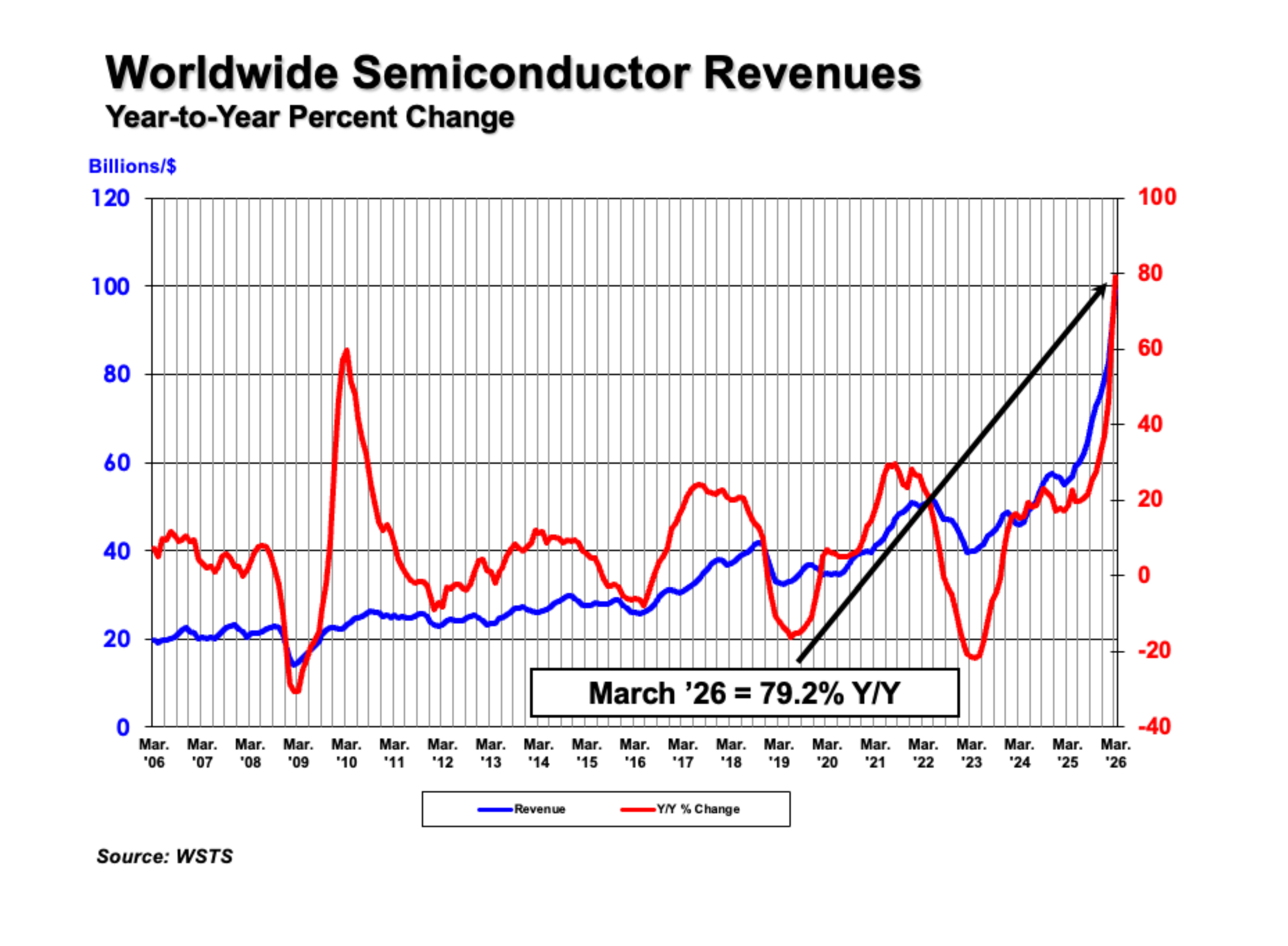
The Semiconductor Industry Association (SIA) today announced global semiconductor sales were $298.5 billion during the first quarter of 2026, an increase of 25% compared to Q4 of 2025. Global sales we
Texas Instruments (TI) reported robust results for the first quarter of 2026 on April 23, driven by surging AI data center demand and a notable rebound in industrial control applications. TI stressed


