
After a two-year hiatus, Samsung Electronics is reportedly set to resume construction of its advanced semiconductor production facility, the P5 fab, located in Pyeongtaek. With continuous improvements in high-bandwidth memory (HBM) and next-generation DRAM technologies, alongside strong market growth expectations for AI semiconductors over the coming years, Samsung is preparing to launch a new round of equipment investment in South Korea.
According to Seoul Economic Daily, Samsung executives are discussing the engineering and investment restart for the P5 fab. Some personnel have already entered the construction site to reorganize materials and begin preparatory work. Industry insiders estimate that large-scale deployment of heavy machinery could start as early as October 2025.
The P5 fab is Samsung's Device Solutions (DS) division's fifth wafer fabrication plant. The multi-story structure covers an area of 650mx195m, with total investments expected to exceed KRW30 trillion (approx. US$22.1 billion). It will become a complex fab integrating multiple production lines, including DRAM, NAND flash, and foundry services. TrendForce reported that it will also house multiple cleanrooms (estimated to be eight), significantly expanding on the four-room designs of P1–P4.
Samsung had initiated foundational work on the P5 fab back in 2023 but abruptly halted progress in early 2024. At that time, the DS division was hit hard by weak memory demand, posting revenues of only about KRW66.6 trillion—a sharp 32.3% decline year-over-year—and recording losses around KRW14.9 trillion.
Lagging technological capabilities also contributed to the pause in investment. Samsung fell behind competitors in both the HBM and foundry sectors, losing technology leadership. Consequently, the company shifted focus toward revising product roadmaps and redesigning products rather than expanding manufacturing capacity.
Recently, however, core products such as sixth-generation 10nm DRAM and fifth-generation HBM3E have seen technical performance rebound. Samsung has begun considering restarting P5 fab construction within 2025. Expectations of sustained AI semiconductor demand further fuel this renewed investment momentum.
According to BusinessKorea, this shift aligns with a broader industry trend: TSMC and SK Hynix are also investing heavily in cutting-edge memory and foundry capacity. Samsung's P5 is positioned to serve both internal DRAM/flash needs and contract foundry services.
Data from the Export-Import Bank of Korea projects the AI semiconductor market size to grow from US$41.1 billion in 2022 to US$133 billion in 2028. Notably, the P5 fab is also scheduled to commence operations in 2028.
Based on this positive technology trend, Samsung plans to accelerate exterior construction of the P5 fab in 2026 and install multiple semiconductor equipment sets in vacated spaces at the P4 fab in Pyeongtaek.
Industry forecasts suggest Samsung will expedite development of the Yongin semiconductor campus in South Korea and may even bypass building a P6 fab, opting instead to initiate construction first at Yongin following completion of P5.
Regarding these reports, a Samsung representative stated that the company is currently analyzing and evaluating the potential restart of P5 fab construction.


Stay up to date with the latest in industry offers by subscribing us. Our newsletter is your key to receiving expert tips.
Texas Instruments (TI) reported robust results for the first quarter of 2026 on April 23, driven by surging AI data center demand and a notable rebound in industrial control applications. TI stressed
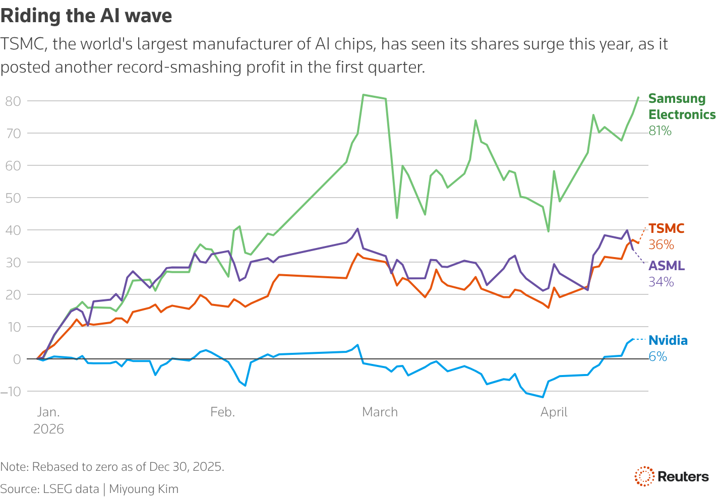
TSMC opens new tab, the world's main producer of advanced AI chips and a major supplier to Nvidia, opens new tab, on Thursday posted a 58% jump in first-quarter profit to record levels that handi
The most valuable technology company in Europe, ASML, reported on Wednesday that the ongoing expansion of AI infrastructure has significantly enhanced its bottom line.The Dutch firm delivered net prof


