The rapid development of AI, HPC, and other technologies is driving higher demands for semiconductor performance and energy efficiency. Traditional packaging technologies struggle to meet the needs of the AI era, creating an opportunity for advanced semiconductor packaging technologies to shine.
This has attracted many leading semiconductor companies to invest heavily in the field. Recently, Broadcom announced new advancements in advanced packaging technology.
Broadcom Introduces the First 3.5D F2F Packaging Technology to Meet AI Computing Demands
Broadcom recently unveiled its 3.5D eXtreme Dimension System-in-Package (XDSiP) platform on its official website. This marks the industry’s first 3.5D F2F packaging technology, integrating over 6000mm² of silicon and up to 12 HBM memory stacks into a single package. This technology meets the high-efficiency and low-power requirements of AI chips.
Broadcom highlighted that the emergence of new and increasingly complex large language models (LLMs) necessitates 3D stacking to achieve better form factor, power, and cost efficiency. The 3.5D integration technology, which combines 3D silicon stacking with 2.5D packaging, is poised to become the preferred choice for next-generation XPUs over the next decade.
Broadcom’s F2F technology directly connects the top metal layers, providing dense and reliable connections with minimal electrical interference and exceptional mechanical strength.
Broadcom stated that it collaborated closely with customers, leveraging TSMC’s technology and EDA partners’ tools to develop the 3.5D XDSiP platform. By vertically stacking chip components, this platform allows chip designers to select the optimal fabrication process for each component while reducing interposer and package size, significantly improving performance, efficiency, and cost.
Currently, Broadcom is developing over five 3.5D products. Most of its consumer AI customers have adopted the 3.5D XDSiP platform and plan to begin mass production shipments in February 2026.
AI Boom Sparks Advanced Packaging Innovations
The surge in AI has driven the emergence of advanced packaging technologies, drawing significant investment from many companies. In addition to Broadcom, TSMC, Samsung, ASE, and Intel are also actively advancing the development of these technologies.
TSMC: Pioneering Advanced Packaging with CoWoS and SoIC
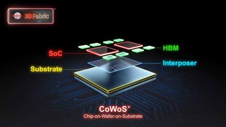
TSMC’s CoWoS advanced packaging technology has gained significant market attention. The company is also heavily investing in developing its SoIC packaging technology. TSMC has integrated its packaging processes into a 3D Fabric system consisting of three parts: the SoIC series for 3D stacking technology, the CoWoS series for advanced packaging, and the InFO series.
SoIC, introduced in April 2018, represents a next-generation packaging innovation combining CoWoS and Wafer-on-Wafer (WoW) stacking technologies. It allows TSMC to directly produce 3D ICs for clients.
This technology began small-scale production in 2022, and TSMC plans to expand its capacity by over 20 times by 2026. Furthermore, reports in November revealed that TSMC has secured a 30-hectare area in Southern Taiwan Science Park to establish an advanced supply chain zone focusing on advanced packaging, supporting future CoWoS/SoIC production at its Chiayi (AP7) and Tainan (AP8) facilities.
Samsung: Developing 3.3D Advanced Packaging for AI Chips
In July, Samsung Electronics announced it was developing 3.3D advanced packaging technology for AI semiconductor chips. Samsung’s concept involves vertically stacking GPUs (AI computing chips) and LCC caches into a single unit interconnected with HBM memory. A silicon bridge chip directly connects the die, and a transparent medium replaces the costlier silicon interposer in the copper RDL redistribution layer.
This design reduces production costs by 22% without compromising chip performance. Additionally, Samsung plans to incorporate panel-level packaging (PLP) into its 3.3D technology. Large rectangular substrates will replace the limited area of circular wafers, further improving packaging efficiency.
ASE: Advancing Chiplet Interconnect Technology
In March, ASE announced new chiplet interconnect technology to address the diverse chip integration designs and advanced packaging needs arising from AI development.
This technology uses microbump technology with novel metal stacking to significantly reduce the interconnect spacing between chips and wafers. ASE noted that enhancing chiplet-level interconnect technology expands its application to AI chips, mobile application processors, MCU microcontrollers, and other key chips.
Intel: Scaling Up 3D Foveros Technology
In January, Intel announced that its 3D Foveros advanced packaging technology had entered mass production at its Fab 9 facility in New Mexico, USA. Foveros technology integrates two or more chips with horizontal and vertical interconnects, reducing bump spacing. This approach improves latency and bandwidth by stacking memory over active components.
The technology divides products into smaller chiplets or tiles, with I/O, SRAM, and power delivery circuits fabricated on the base die, while high-performance logic chiplets are stacked on top.
Foveros enables ultra-low-power, high-density chip interconnects, minimizes partitioning overhead, and allows rational selection of chip processes for each block. This enhances cost and performance, simplifies SKU creation, and accelerates time-to-market.
Stay up to date with the latest in industry offers by subscribing us. Our newsletter is your key to receiving expert tips.

The semiconductor industry is bracing for further disruptions as China steps up efforts to ensure the stability of its semiconductor supply chains, according to a Reuters report. In a move aimed at mi

hina's National Development and Reform Commission (NDRC) has issued a rare monitoring report warning that rising memory prices are spreading across the electronics supply chain as tight supply and

Nvidia strengthened its dominance in the add-in-board (AIB) GPU market in the fourth quarter of 2025, capturing a record 94% market share even as overall shipments dipped amid rising memory prices and