Resasas has put its in-house developed 32bit RISC-V core into a few-pin general-purpose MCU series, following earlier RISC-V projects with Anders and SiFive.
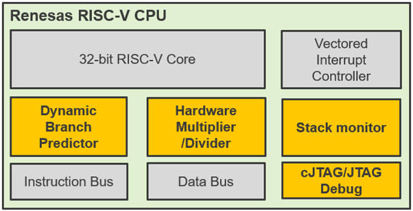
Announced last November, the core implementation can accommodate various standard RISC-V options, to which Renesas has added its own options including: a stack monitor register to protect against rogue software, a dynamic branch prediction unit improve the average execution throughput, and a context-saving register bank to speed interrupt response.

Two-wire compact JTAG debug can be implemented for low pin-count packages, and performance monitor registers can be added for benchmarking, as well as an instruction tracing unit.
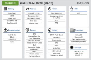
The new microcontrollers, called the R9A02G021 group, come in packages with between 16 and 48pads: 2 x 2mm 16pad WLCSP and QFNs from 4 x 4 to 7 x 7mm with 24, 32 or 48pads – there is one part number for each of the four packages.
They implement the RV32I instruction set and include two-wire JTAG and the company’s core-local interrupt controller (CLIC)
Clocking is at up to 48MHz, delivering 3.27Coremark/MHz, and consumption is 162μA/MHz, or 300nA in stand-by with 4μs wake. Operation is over 1.6 to 5.5V and -40 to 125°C.

There is 128kbyte of instruction flash, 4kbyte of data flash and 16kbyte of ram, plus a 12bit ADC, an 8bit DAC and serial communication including UART, SPI and I2C.
The company’s ‘SAU’ peripheral is also included to implement up to six simplified SPI interfaces, up to three more UARTs or up to six simplified I2C interfaces, depending on package size.
To tempt potential adopters from more familiar architectures, Renesas has lined up plenty of support from the start, with the its e2 studio Eclipse-based IDE (integrated development environment) providing a code configurator and the LLVM compiler.
“Complete development environments are also available from IAR with its Embedded Workbench IDE and I-jet debug probe, and Segger with the Embedded Studio IDE, J-Link debug probes and Flasher production programmers,” it said.
FPB-R9A02G021 is the hardware development board (right).
No less than 18 application notes have been prepared to go along with the product launch, covering state-switching, boot firmware and many of the peripherals.
Stay up to date with the latest in industry offers by subscribing us. Our newsletter is your key to receiving expert tips.

hina's National Development and Reform Commission (NDRC) has issued a rare monitoring report warning that rising memory prices are spreading across the electronics supply chain as tight supply and

Nvidia strengthened its dominance in the add-in-board (AIB) GPU market in the fourth quarter of 2025, capturing a record 94% market share even as overall shipments dipped amid rising memory prices and

Broadcom shares rose sharply in aftermarket trade on Wednesday after the artificial intelligence chips maker delivered a quarterly top and bottom-line beat and provided current quarter revenue guidanc