Infineon announced that it has succeeded in developing the world's first 300mm GaN wafer technology for power electronics. This allows for the improvement of efficiency performance, smaller size, lighter weight, and lower overall cost for the chips.

According to Infineon, the breakthrough will help the company to significantly advance the market for GaN-based power semiconductors. Chip production on 300-millimetre wafers is technologically more advanced and much more efficient than on 200-millimetre wafers, as the larger wafer diameter enables 2.3 times the number of chips per wafer to be produced. Infineon writes that the new production process “enables efficiency performance, smaller size, lighter weight, and lower overall cost. Furthermore, 300 mm manufacturing ensures superior customer supply stability through scalability.”
Infineon also estimates that being able to use its existing 300 mm silicon manufacturing equipment, “since gallium nitride and silicon are very similar in manufacturing processes. Infineon’s existing high-volume silicon 300 mm production lines are ideal to pilot reliable GaN technology, allowing accelerated implementation and efficient use of capital.”
“This remarkable success is the result of our innovative strength and the dedicated work of our global team to demonstrate our position as the innovation leader in GaN and power systems,” said Jochen Hanebeck, CEO of Infineon Technologies AG. “The technological breakthrough will be an industry game-changer and enable us to unlock the full potential of gallium nitride. Nearly one year after the acquisition of GaN Systems, we are demonstrating again that we are determined to be a leader in the fast-growing GaN market. As a leader in power systems, Infineon is mastering all three relevant materials: silicon, silicon carbide and gallium nitride.”
Infineon recently also opened a new semiconductor production facility in Malaysia, which focuses on silicon carbide converters. The company has also been researching a semiconductor project with GaN since May 2025.


Stay up to date with the latest in industry offers by subscribing us. Our newsletter is your key to receiving expert tips.

The artificial intelligence(AI) boom is triggering an unprecedented expansion race among the world's largest memory chipmakers.Surging demand for high-bandwidth memory (HBM) and high-performance D
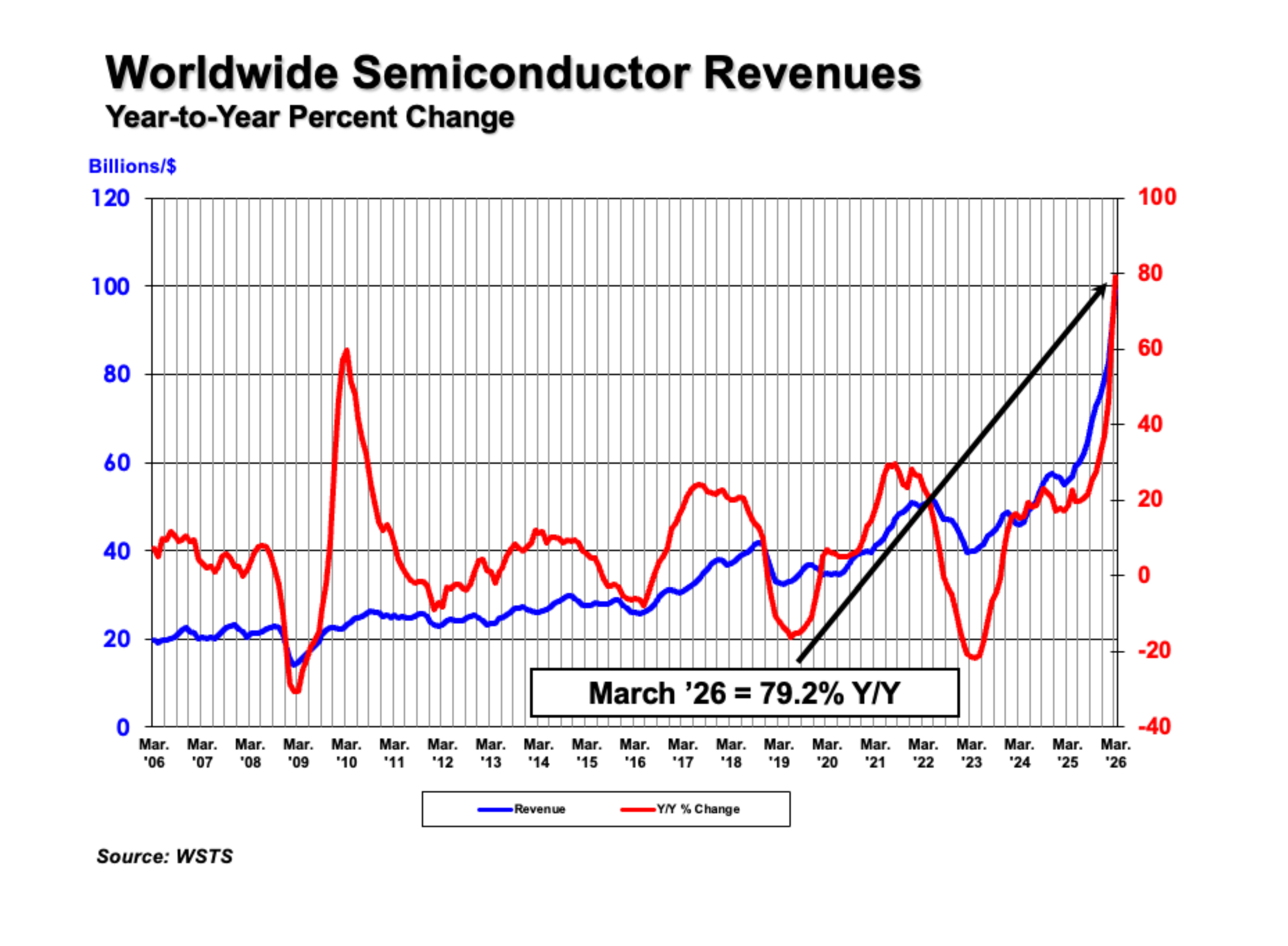
The Semiconductor Industry Association (SIA) today announced global semiconductor sales were $298.5 billion during the first quarter of 2026, an increase of 25% compared to Q4 of 2025. Global sales we

Texas Instruments (TI) reported robust results for the first quarter of 2026 on April 23, driven by surging AI data center demand and a notable rebound in industrial control applications. TI stressed


